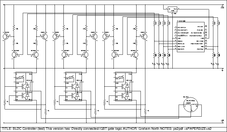
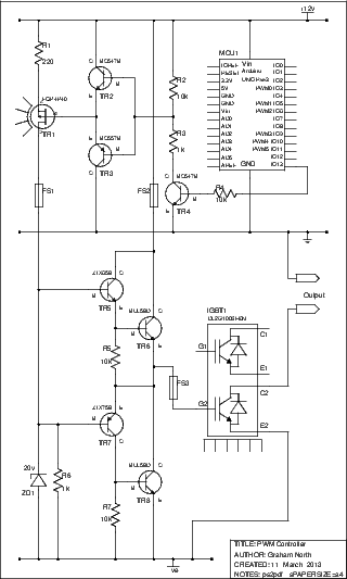
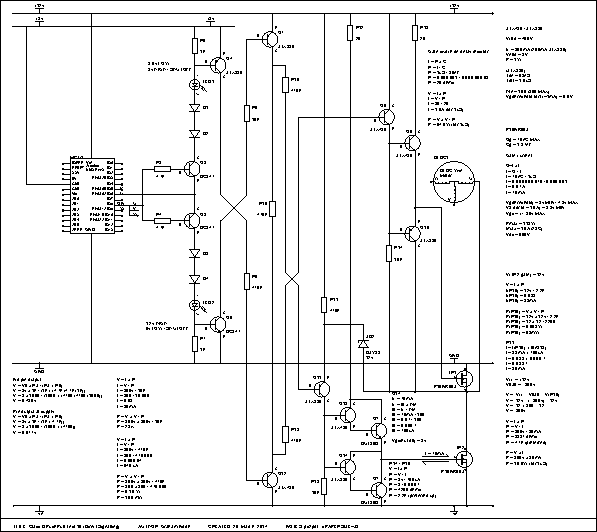
So we have the simple PWM circuit, as above, with the IGBT directly driven from the BC108/KSP94 level changer transistors and a 1k gate discharge
Gate switching speeds are not going to be too hot as the current is not great.
The circuit was powering the milk float motor from a 12v supply (a car battery) in split rail mode.
A charger was attached to maintain the battery charge eventually.
The IGBT were not cooled in any way initially.
Currents were in the 10-30A and the actual voltage was between 11v and 12v.
I'm looking at the motor spinning at a very low speed, probably around 100RPM and the IGBT is steady at 37C
PWM is 225mS period with 30mS mark, so that's 13.33% mark/space and about 4Hz frequency.
The current is 13.8A during the mark so the average current draw is 1.84A.
So before adding the above mods it was worth while testing out a basic controller:
This amazingly simple controller worked a treat on the Prius brushless motor.
The wheels would be turning at an equivalent of about 10mph, but the IGBTs where holding temperatures less than 40C.
This was without any heat-sinking or cooling of any kind.
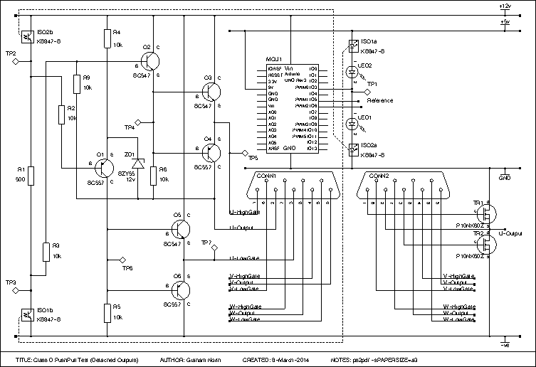
IGBT Controller Initial Test:
Prius Controller Testing (wheels):
IGBT Controller on a Prius:
High Speed Switching
Although the circuit worked, the gate switching was quite slow, about 1mS.
We really need this to be in the order of 1uS.
In order to do this, we need a relatively high current spike into the gate to switch quickly.
This means a current amplifying gate driver circuit.
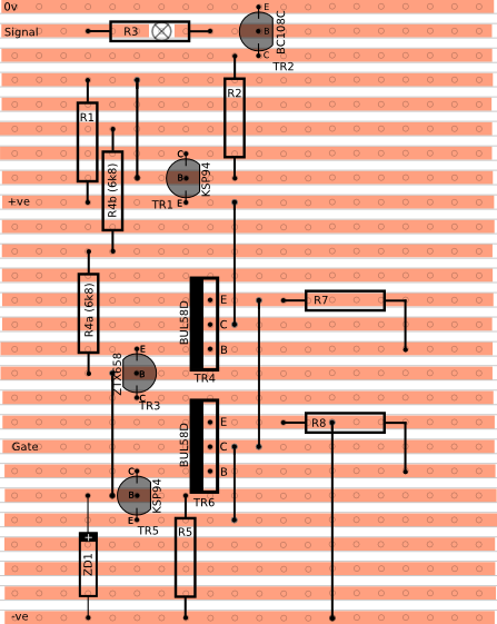
So we are looking at a complimentary emitter follower driver.
This will have to be a 2-stage circuit in order to keep low current in the logic circuit.
The concern here is that the gates will not be completely switched off,
just down to 1.5v due to the base bias.
This is well below the 8v or so "on" voltage of the IGBT gate, so really we are OK.
Further research shows that a Sziklai pair (using one PNP and one NPN) reduces the base voltage to 0.7.
This is because it cannot rise to more than 0.7 v below supply.
This is fine since it's function is only to sink the gate.
It means we can use two identical high power NPNs for gate swtiching and a PNP/NPN pair to drive these.
Also use of 10k switch off resistors on the intermediate bases will speed switch off times,
and we can add a zener to the input to cap the gate below 20v.
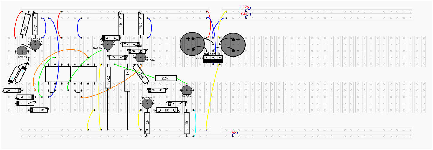
Layout on stripboard. Here we are using 2 x 6k8 7W resistors for R4 since they are stock.
Three versions of this circuit were actually tested:
First a low voltage version using 12v for the motor power.
There was some issues at first, but these were due to layout, but the circuit functioned as expected.
This was using a 470R resistor for R4 so the base current was high enough to switch.
Direct Gate Controller PWM Test 1
Direct Gate Controller PWM Test 2
Next test was a high voltage test with an original MK2 Prius battery and the load was a 240v 500W lamp.
This was with 2x6k8 resistors in series (13k6 total).
Again the circuit performed as expected with switching speeds in the microseconds to nanoseconds.
Direct Gate Controller High Voltage PWM test
The final test was to put the IGBT in high side mode just to confirm it works as expected, which it did.
Direct Gate Controller High Side Test
Gate switch voltage was around 20v for low side (both low and high voltage)
and showed around 6v for high side (high voltage only tested)
Only observed the switch off times which were between 15uS and 20uS.
Can probably tune this down to the target 1uS by tuning the base switch resistors R4 and R6.
Component Availability
The problem with the timing was inspected more closely and the mark was 1uS - 2uS, which is fine,
but the space is 10uS - 20uS and there is a delay.
This problem has been met before when a MJ2955 was used.
It's due the component switching times, in this case of the KSP94.
There is no published switch speed or transition frequency for the KSP94,
But the details of the NPN counterpart the KSP44 is around 10MHz.
The switch on is using ZTX658 + BUL58D and gives low switch times.
There is the ZTX758 which is the PNP version of the ZTX658 so this has been sourced as an upgrade of the KSP94.
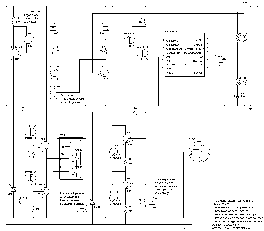
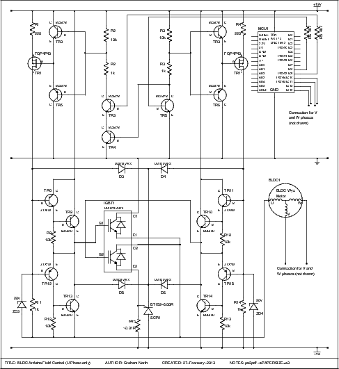
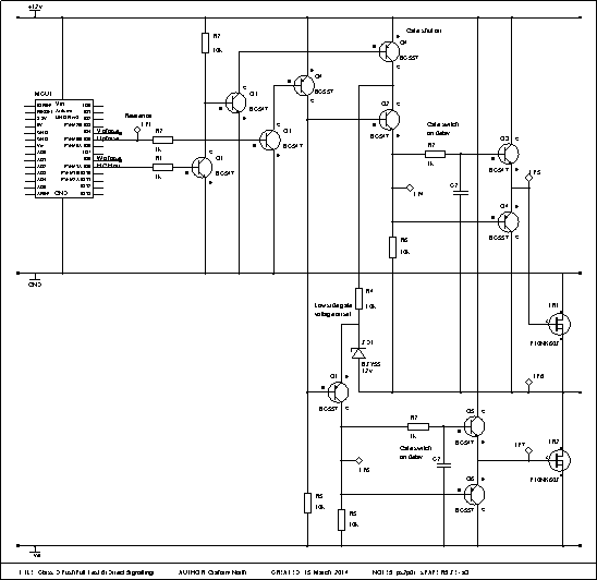
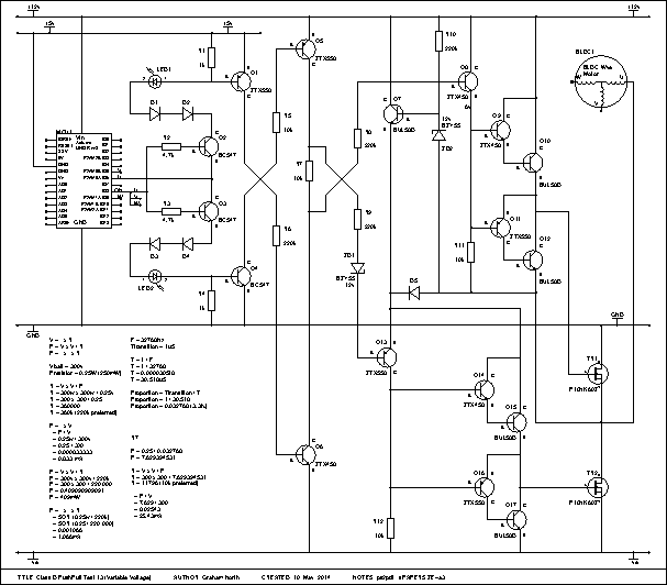
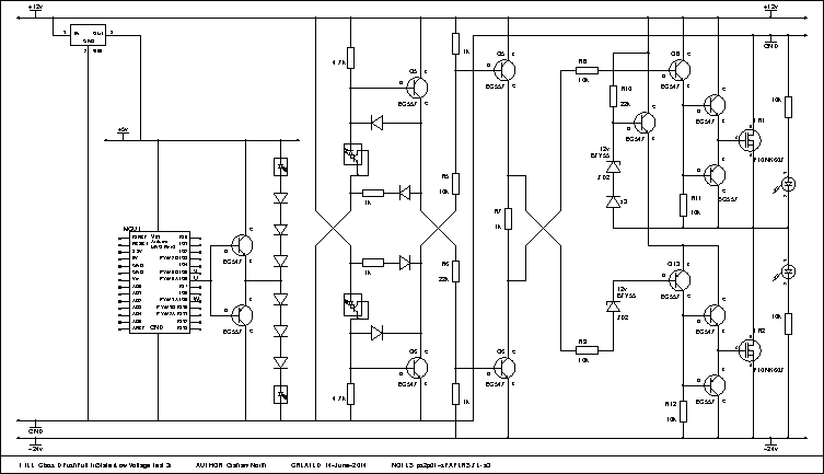
Constructing the Full Controller
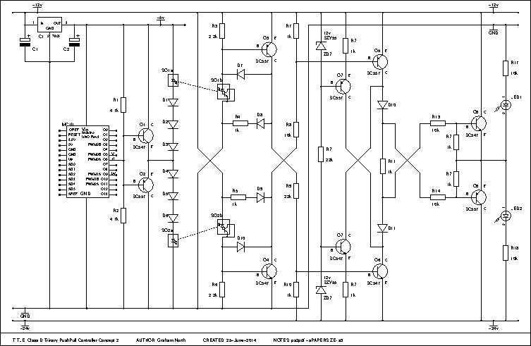
Revised glitch protection, shoot through protection also adding the current source circuits:
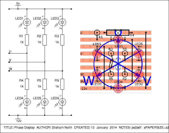
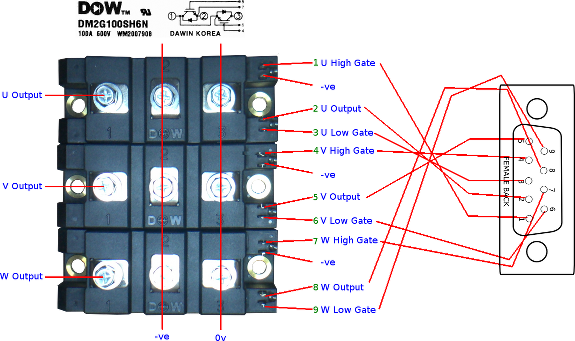
This circuit is just a single phase (phase U) and would be replicated for the other 2 phases.
This includes all the protection circuits and can power a high voltage motor with the right IGBTs.
This version has:
Directly connected IGBT gate drivers - all switching times 500nS or less.
Shoot through lockout harness - clamps all drivers full gate discharge to release shoot through in <100nS on detect of avalanche current.
Universal software gitch safe driver logic - impossible for software to cause shoot through.
Gate voltage clamp for high voltage operation - gate voltage clamped to +/-20v no matter what the battery state.
Current source regulators for stable gate drive - stable (dis)charge rate maximising switch speed and limiting EMC.
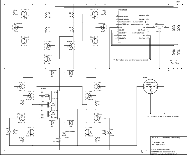
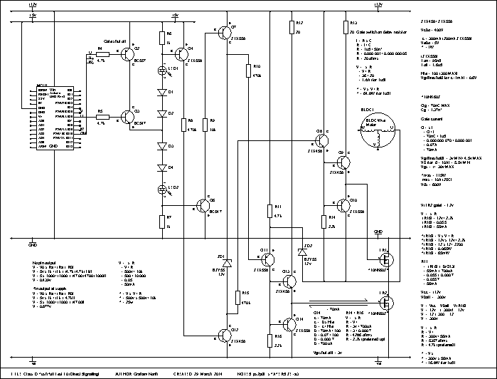
Revised the current source circuits to MOSFET based:
The most expensive part of the controller is the IGBT, which in this case was originally sourced as a match to the original Prius IPM.
The IPM in the Prius is 600v/600A/1790W part specifying for 20kHz switching are around £1,000.
The IGBTs currently used are 1200w/450A/2080W tested up to 1MHz switching frequency and are around £200 each module so £600 total.
The 3 parameters are
the voltage, set by the input voltage,
the current, drawn by the windings on full power,
and the power dissipation which is the average power through the IGBT during transitions.
Voltage is the low rail of supply which for testing will be the Prius battery voltage (273v).
Current is the maximum drawn in the windings (for a 30kW motor is going to be around 100A).
The power dissipation relies on the pwm frequency and the switch speed.
The switch speed is assumed to be our target switch speed of 1uS, which we should achieve in the implementation above.
The PWM frequency in this controller is variable proportional to the vehicle speed, so the maximum is governed by the top speed of the vehicle.
If we calculate for a speed of 100mph, use the dimensions of our Prius front wheels and Daihatsu HiJet diff ratio 40/9 (4.44:1).
Also for our Prius BLDC motor we have 4:1 field to shaft rotations.
Converting: 1 mph = 0.44704 ms-1
so 100mph in metres per second is:
100 * 0.44704 = 44.704m/s
Diameter of Prius front wheel is: 0.55m by rough measurement which is 0.55π circumference so 1.7279, so rotations per second is:
rps = 44.704 / 1.7279 = 25.872
So 26 revs per second would give us about 100mph.
Gears give us 4.44:1 so need 114.87 rps at the motor shaft,
and 4:1 electrical to physical gives about 460 (459.49) field rotations per second for 100mph.
For one rotation in the 12 step sequence there are 10 transitions on a single IGBT (5 steps by 2 edges, and then 7 off states).
So there are 4,600 transitions per seconds where the IGBT is neither on nor off (power is being dissipated) and these last for 1uS max.
So the IGBT spends is 4,600 x 1uS = 4.6mS per second (about 0.46% time) dissipating 30kW of power giving an average dissipation of:
30000 * 0.0046 = 138w (in theory).
At high power (but less than full power) we could also switch to a 6-step sequence which would be 4 transitions, so:
138w * 4 / 10 = 55.2w
So an air heatsink only will be required as we are only dissipating a moderate amount of heat.
A processor heatsink would be enough to maintain the lowest thermal band and get the most out of the parts.
Compare this with a fixed PWM frequency around 15kHz (used in the Prius), which is 30,000 transitions per second of 1uS each.
This means the IGBTs have to dissipate 30mS in 1,000mS or about 3%.
3% of 30kW is 900w, which is a serious heater and no wonder there is a liquid cooling system to dissipate it!
All these things mean we can source a part requiring to withstand only a fraction of the approx 2kW dissipation and at a considerably lower cost too.
Obviously at low speeds, e.g. around town etc,
the controller PWM frequency is a fraction of even this so the dissipation is extremely low even under full power.
We can also arrange for the software to switch to a lower step sequence on increasing shaft speed (and also temperature)
to maintain low power dissipation and maintain a dissipation budget.
Indeed in some of the more expensive controllers they do indeed switch to lower PWM frequencies for lower shaft speeds,
but they have tested this in cars and found that users complain of the whine.
In the Mass-EV the frequency will be linear with the shaft speed just like in piston engined cars, which is acceptable.
The only other thing to consider is the max current a low PWM when starting from stationary which is only limited by the resistance of the windings.
At higher RPM it is limited by back EMF also.
The specific device being considered has a short circuit withstand time of 10uS,
so clearly the device can withstand shoot-through currents (which are massive) for short periods.
Also the design of the controller has a short circuit protection SCR which would shut off the IGBTs in the event of over-current in around 3uS.
This is updated to include the Arduino board and the new £25 IGBT modules:
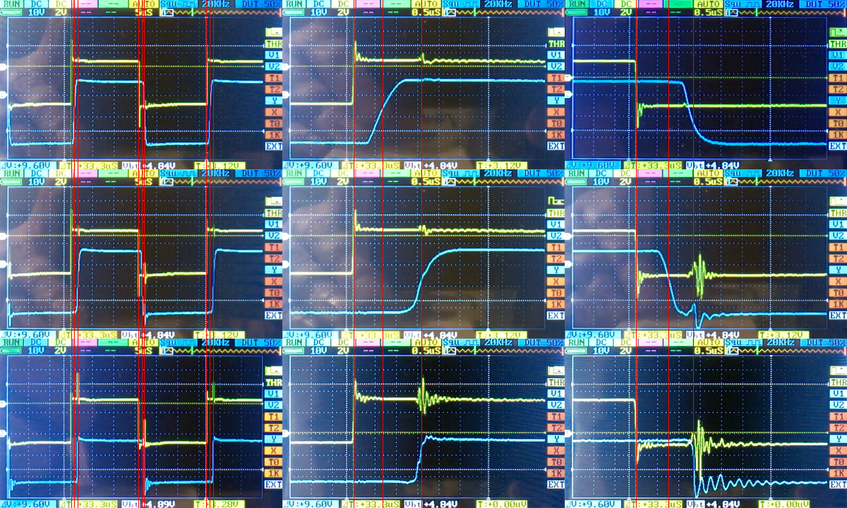
This was built and both rise and fall times on the IGBT gates were 800nS.
This was tested with the negative supply rail at -12v.
Next we need to test at -300v.
Regenerative braking
Need to work out the current load on the back EMF diodes as we may need to add more diodes.
This is only a temporary workaround for the permanent magnet motor as the Mass-EV will have electromagnetic rotors
so back EMF will be controlled electronically.
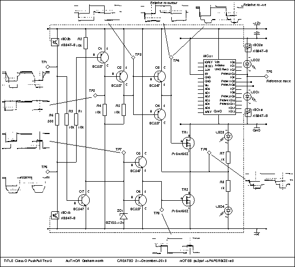
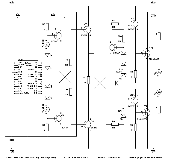
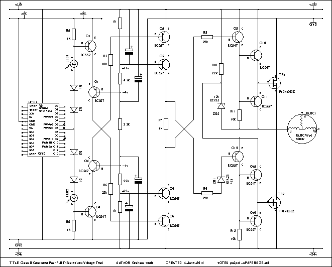
Class-D Push-Pull Controller
This is a new direction for the controller which arose from the HV R&D; testing.
For the electronics this means the MCU is providing only 3 PWM outputs for the 3 Phases.
The standard class-D amplifier is a H bridge or 2 x 180 degree phase outputs which drive the 2 terminals on the speaker.
This is driven by an analogue-to-PWM converter on the input and simply driving the outputs with one inverted.
Thus giving 180 degree phase difference between the 2 half bridge outputs.
To adapt this design, this needs to be extended to 3 x 120 degree half bridge phase outputs.
Each having it's own PWM input from the MCU, which will provide the 3 PWMs at 120 phase angles.
Using optocouplers in push-pull this provides the PWM inputs for the 3 independent channels.
For the motor output a logic high (5v) will give positive feed and logic low (0v) will give negative.
The dead time will be simply provided in the electronics using the propagation delay in the optocouplers.
Obviously, all the complexity in transferring 2 PWM outputs to a single half bridge disappears.
Also as this is a class-D output we do not need to control the gate voltage as this will be controlled by the MOSFET/IGBT output itself
This will be tested on the model motor first with STP10NK60Z outputs which are 600V 10A (36A pulsed)
This circuit was tested without the motor, but it did not work.
It appears the 2 MOSFETs were in shoot-through, but it's not obvious how this is the case.
It may be due to the transition amplifiers being switched against the output.
The circuit is redesigned to have these across the supply rails instead.
A resistor was added between the optcouple outputs to limit the current through them.
The bases of the transition amplifiers have to be connected to the right points to have them switch correctly.
This is being tested using an approx 16kHz square signal from the Arduino.
The mark/space is fully variable and is set to a very rough 50% to see the transitions.
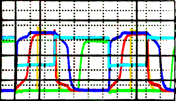
This is a trace of the partially built circuit without the drivers and output:
This is the same where the low side trace is inverted to see the dead zone easier:
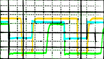
This is after the drivers and outputs are added:
There was an error in the circuit where the optocouple LEDs connected the wrong way round.
This is the reason the input waveform is inverted in the above scope traces.
This was corrected.
There is a problem with the low side not switching properly on so this was reverted
to being switched from the positive rail using a zener to clamp the gate voltage:
Now the low side MOSFET switches on fully and the circuit performs as expected.
Still not happy with the pre-drivers.
Class-D (or any push pull) amplifier should really have all the driver stages in push-pull mode.
This uses the feedback in the circuit to simplify the stages without losing the quality.
The 2 traces for the high side test points TP4 and TP5 are relative to the negative rail (left of the pair),
and relative to the output (right of the pair).
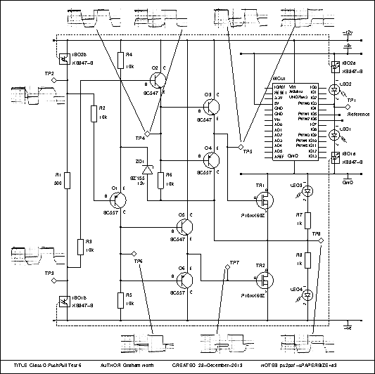
So now we have a good circuit using push-pull for the whole circuit.
This means it will scale up to high voltages well as this uses the feedback to improve the switching times.
The noise seen in the traces is when both output stages are in open circuit so the voltage is not clamped to either rail.
When this is driving a real output this will disappear as the motor phase coil will control the voltage in these dead zones.
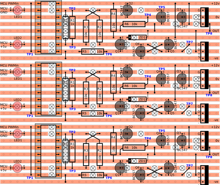
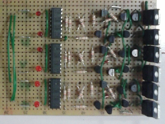
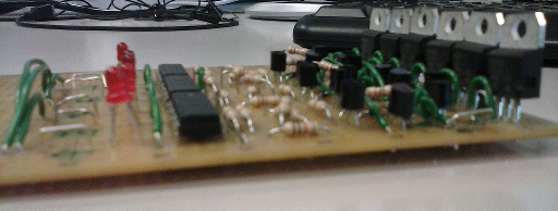
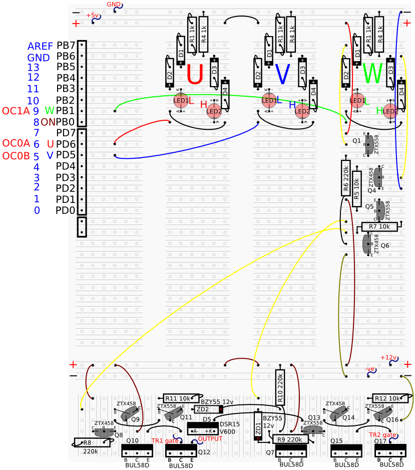
This is the completed 3 channel layout on stripboard:
Credit to Ron J for the inkscape skeleton drawings
Drilling mask:
When the circuit was commited to PCB there were some extra issues:
The circuit has an initial condition which actually puts the outputs in shoot through.
This is because the 2 bases of Q1 and Q2 are connected via R1 R2 and R3.
Since the emitters are at 12v potential difference due to ZD1 this means they will both switch on.
The workaround for this is to add R9 to switch off Q2 when there is no input.
This leaves Q1 turned on and so there output is held down to the -ve rail, but at least it means there is no shoot through.
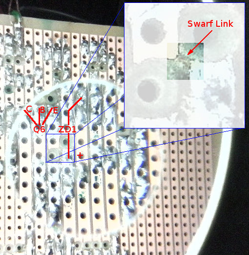
A second issue was due to drilling swarf connecting ZD1 plus inout to Q5 emitter.
This was very difficult to find as it was small and hard to see against the background.
This was only on one channel so was easier to see this was PCB issue and not a design problem.
The swarf was removed and the circuit then worked as the other 2 channels.
This is the finished board:
You can see that R9 is soldered over the top of R6.
Also there are extra wires soldered on to connect the common power rails.
Connections to the board are using crocodile clip loops soldered into the board as with the relay boards earlier.
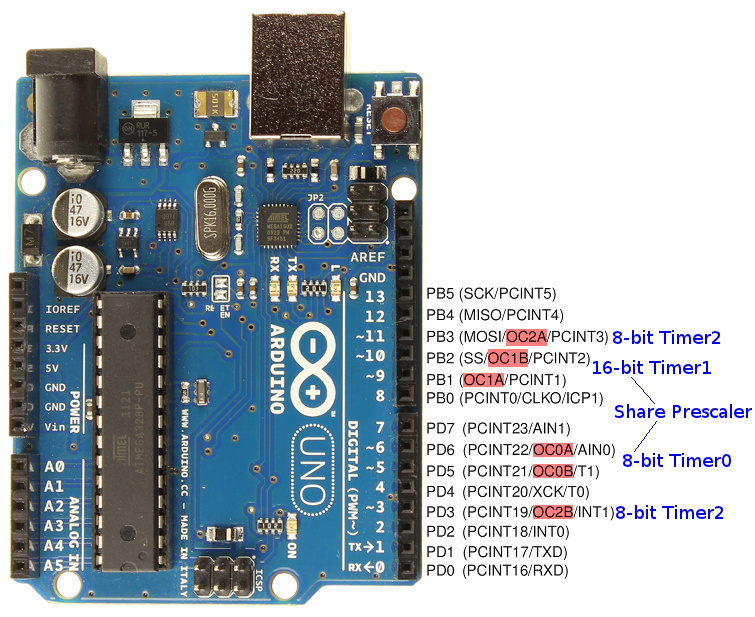
The mapping between the PWM outputs and the pins needs to identified.
ATmega328 have 6 PWMs each of which are paired to a timer.
Timer0 = OCR0A / OCR0B
Timer1 = OCR1A / OCR1B
Timer2 = OCR2A / OCR2B
In the software timers Timer0 and Timer1 share a prescaler so these are best for this.
This gives us 4 PWMs but we only need 3 so both on Timer0 (OCR0A/B, Pins 5/6) and the first on Timer1 (OCR1A, Pin 9) are used.
Class D controller with AC synthesis first open loop test
The opto-isolators are not really useful at high power due to the propogation delay.
This is OK at low voltages since the power is low, but it will not scale to high voltages without complications.
This means the direct gate drive circuit, which has been tested at high voltage, is really the way to go with this.
The isolation is not required as the circuit is robust enough at high voltages.
This is a first pass at this, but it's far from the final to test.
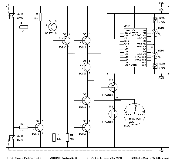
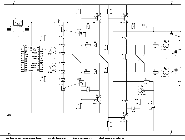
Refining the circuit combining push-pull drive with the class-D circuit using complimentary transistors to switch against opposite supply rails.
Also incorporating the tested high voltage gate driver circuit from the first "BLDC Controller Direct Test"
The above circuit seems to work fine, but there is an issue of the low side MOSFET not really being switched hard on.
So the circuit was redesigned to shut off the low side charge supply when it is not charging the low side MOSFET.
Also the common emitter parts of the circuit are modified to control the open circuit base voltage to around 1v.
This greatly improves switching times.
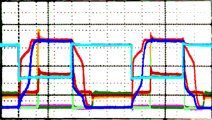
TOP:high side of R7
MIDDLE:low side of R7
BOTTOM:output
The traces around R7 show 2uS delay and around 0.5uS transition for both high-to-low and low-to-high.
The slopes on the output are due to the 10k resistors limiting the discharge current in the discharge transistors.
Also the low side discharge is shortened
This is because of the low side charging supply being switched from the +5v rail instead of the +12v
There is also a significant amount of noise on the input signal.
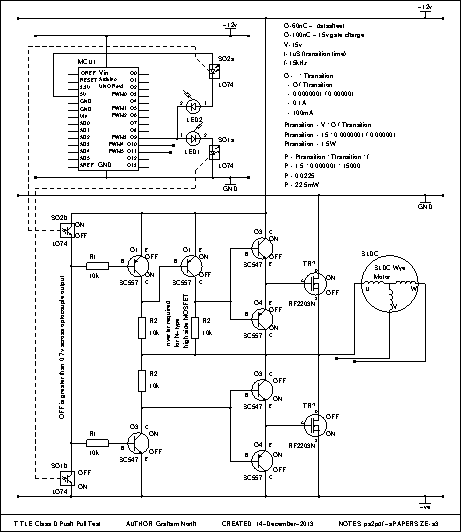
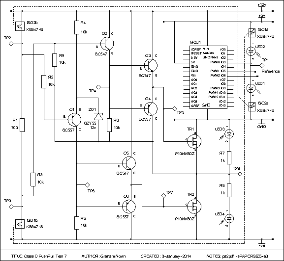
Moving on from the binary output, which just gives us high-low output, the third state -off- is now used in the software.
This is a 3-state or trinary logic controller, since all 3 states are used to drive the output.
This is not tri-state as this is where outputs are switched off to allow other devices to use a common bus.
Trinay logic makes it impossible for the MCU to produce the shoot through condition.
This presents new challenges as there is actually no "pull" part when switching single sided.
The original class-D circuit relies on the push-pull of Q5-R7-Q6 to give us the fast switching and output crossover timing.
The most logical way to do this would be to use the analogue port as only 2 of the 6 pins are in use.
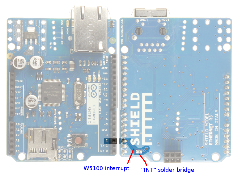
Moving the sense to the analogue port frees the SD card slave select and interrupt pins
Even though the SD card is not used it will interfere with the controller.
Also the W5100 SPI slave select is shared with the gate shut off so this is moved to pin 8 (PB0)
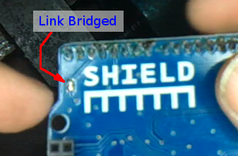
The actual "INT" label they describe in the documentation somehow is no longer on the PCB,
but tracing the circuit shows this is quite obviously the bridge point.


